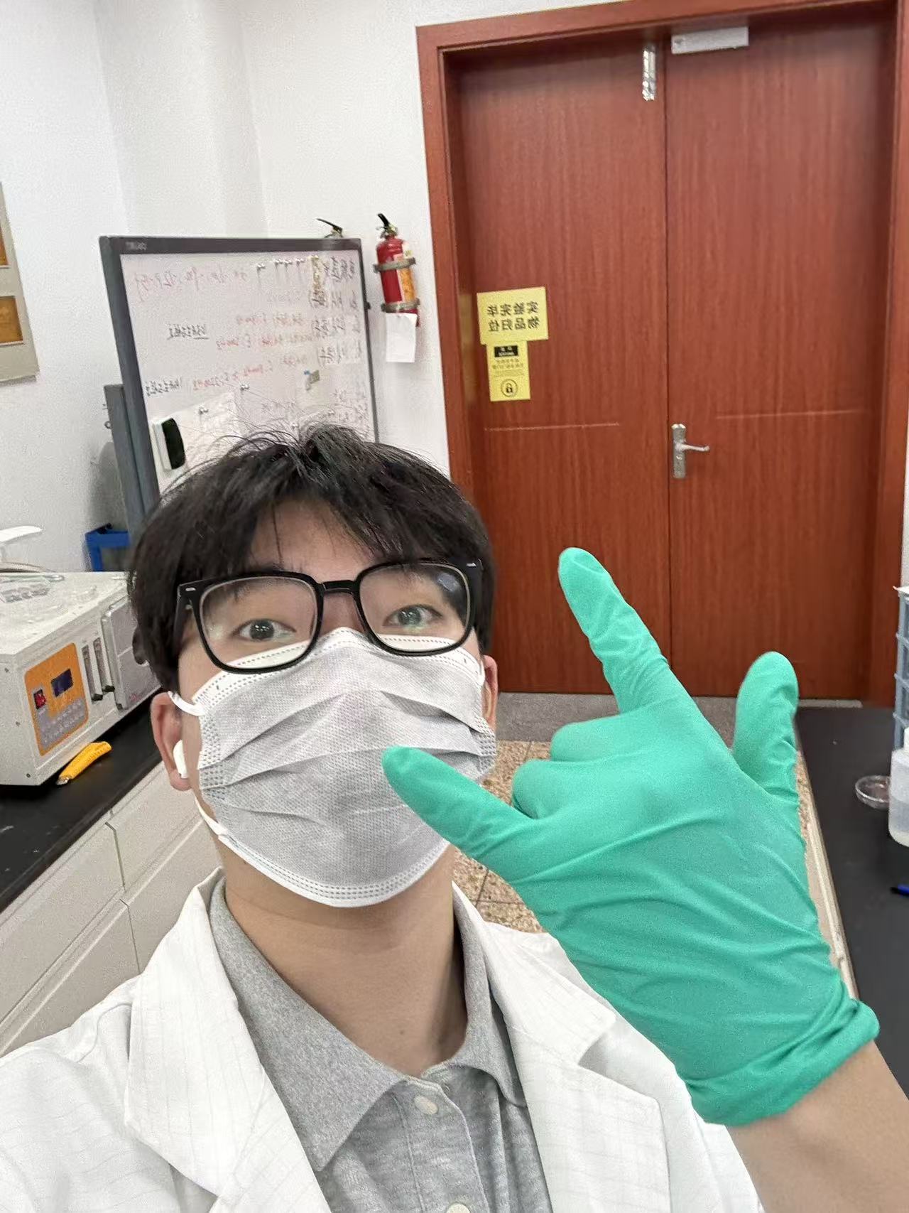
Physics, Integrated Circuit Devices & Physics
Shaoxing University. Current research direction: neuromorphic devices, emerging dielectrics, and AI-assisted semiconductor research.
绍兴大学 2025 级物理学研究生,研究方向为集成电路器件与物理,聚焦神经形态器件与新型介质材料。
Neuromorphic Devices / IC Device Physics / AI-assisted Research
A physics graduate student in Shaoxing University's 2025 cohort, focused on neuromorphic devices, emerging dielectrics, and AI-assisted semiconductor research.
绍兴大学 2025 级物理学研究生,聚焦神经形态器件、新型栅介质与 AI 辅助半导体科研。
Leo Lou works at the intersection of physics, integrated-circuit device research, and AI-assisted scientific workflows. The profile frames his work through research questions, device concepts, and the transferable toolkit he is building for semiconductor industry roles.
Leo Lou 的研究定位连接物理学、集成电路器件与 AI 辅助科研,重点呈现研究方向、器件思维与面向半导体产业的可迁移能力。
Education & coursework
本科毕业于绍兴大学微电子相关专业方向,目前为绍兴大学 2025 级物理学研究生,研究方向为集成电路器件与物理。
Shaoxing University. Current research direction: neuromorphic devices, emerging dielectrics, and AI-assisted semiconductor research.
绍兴大学 2025 级物理学研究生,研究方向为集成电路器件与物理,聚焦神经形态器件与新型介质材料。
Shaoxing University. Undergraduate training established the circuit, semiconductor, process, layout, and testing foundation for device-oriented research.
本科阶段完成微电子科学与工程相关训练,形成电路、半导体物理、工艺、版图与测试基础。
半导体物理、半导体器件物理、高等量子力学、薄膜物理。
集成电路工艺原理、集成电路工艺实验、集成电路制造、半导体器件封装。
电路分析基础、数字电子技术、电子线路、EDA 技术、集成电路版图设计。
半导体光电材料、光伏器件与技术、集成电路分析测试技术。
Operating modes
Click a mode to view Leo from an academic, technical, or industry-facing lens.
01
Focused on emerging memory devices, ion-regulated interfaces, and artificial-synapse-oriented device concepts within integrated circuit device physics.
Research layer
研究主线围绕神经形态存储、离子调控界面与可持续器件材料展开,面向低功耗存储与未来计算硬件的器件探索。
Exploring device behaviors that move beyond binary storage toward synapse-inspired response, adaptive modulation, and low-power computing relevance.
类突触响应、多态调控与低功耗存储相关器件行为。
Studying how electrolyte and bio-derived dielectric systems may enable stronger interfacial modulation and richer device response.
电解质与生物衍生介质对界面调控和器件响应的影响。
Considering environmentally conscious, low-cost, flexible, and process-accessible materials as part of the next generation of electronic devices.
绿色、低成本、柔性兼容与工艺可接近的新型材料体系。
Current projects
The projects are presented through research problems, device-level advantages, and potential application value, with emphasis on material-device coupling, ion modulation, sustainability, and process accessibility.
Experimental toolkit
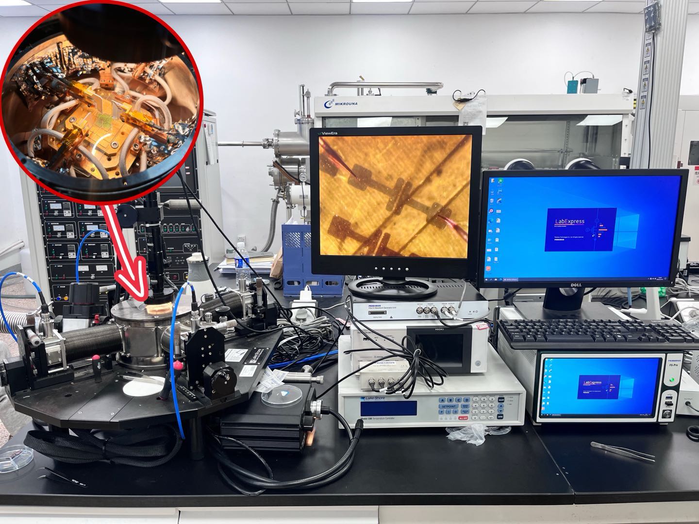
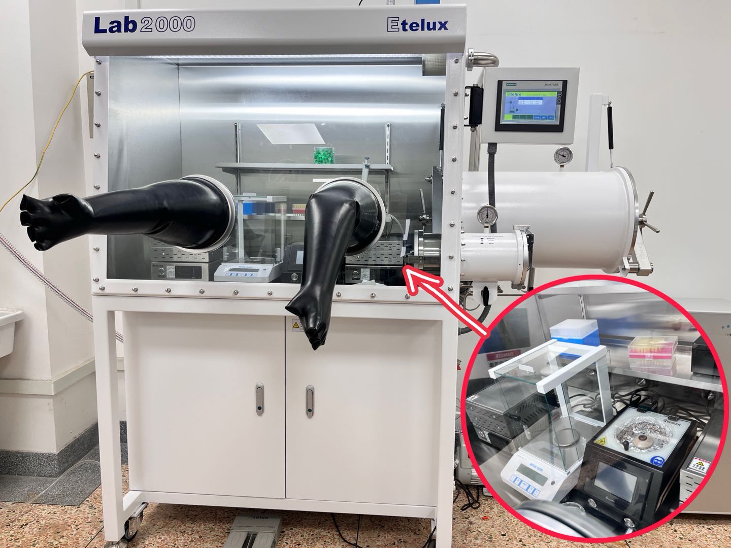
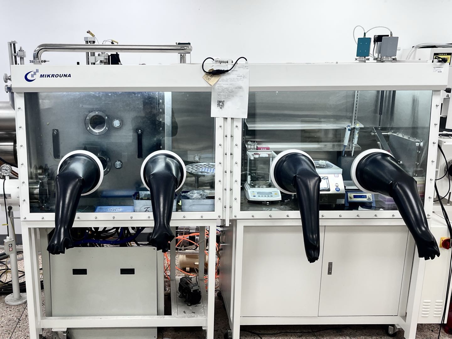
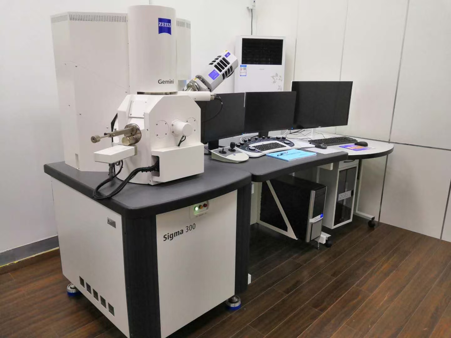
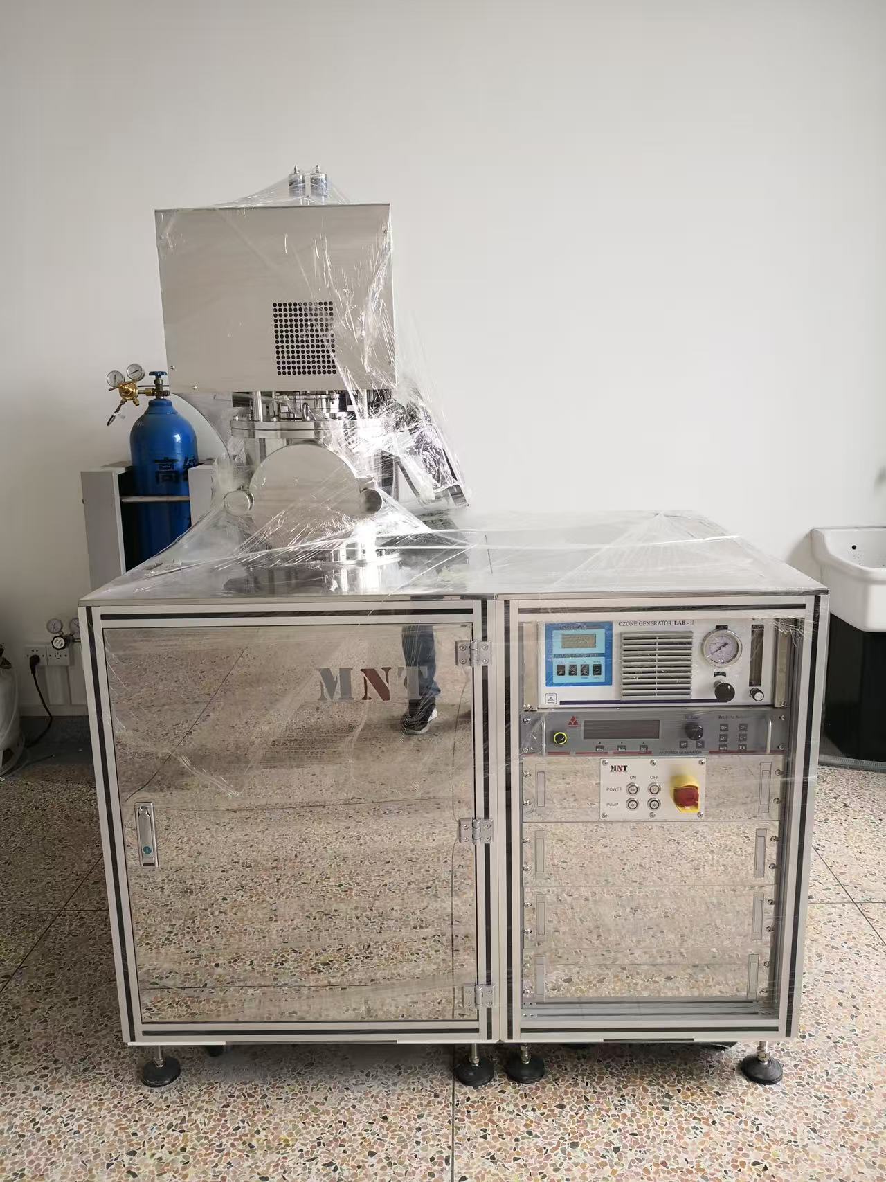
覆盖薄膜制备、电学测试与 SEM / XPS / XRD 等材料表征,可服务于器件研发、PIE 与工艺 PE 相关岗位。
Publication
Haoliang Lou is the fifth-listed co-author of this peer-reviewed work on a low-voltage photoadaptive organic synaptic transistor for autonomous neuromorphic vision.
该论文发表于《Nano Letters》,娄浩樑为第五作者。研究聚焦用于自主神经形态视觉的低电压光自适应有机突触晶体管。
DOI: 10.1021/acs.nanolett.5c05834Career direction
职业目标聚焦器件研发、工艺整合工程(PIE)与工艺工程(PE),以物理背景和器件研究能力作为核心竞争力。
Emerging memory, neuromorphic devices, dielectric systems, electrical response analysis, and device physics interpretation.
Process integration thinking across thin films, dielectric stacks, interface behavior, device response, and materials-informed troubleshooting.
Hands-on familiarity with spin coating, evaporation, sputtering, ALD, probe-station measurement, and parameter-analysis workflows.
Resume
Two resume versions are available: a Chinese version for domestic semiconductor applications and an English version for international or bilingual contexts.